![]()
|
|
|
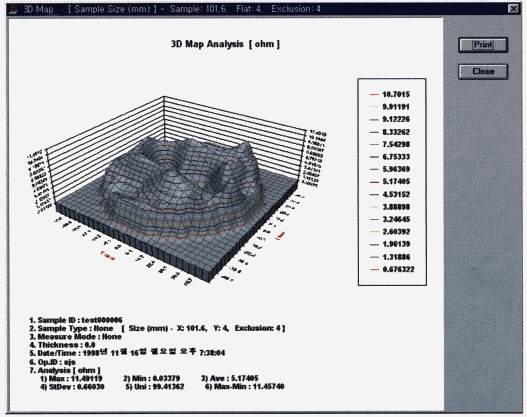
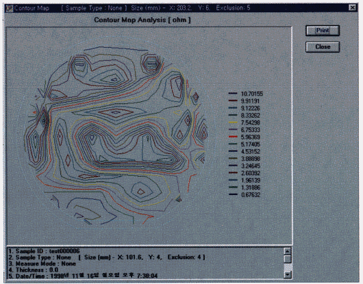
| Automatic Mapping Four Point Probe System Materials Development Corporation offers the complete line of Four Point Probe systems from AIT. Systems are available to measue up to 12" diameter (300 mm) wafers as well as specialty systems for Photovoltaic wafers and substrates. For more information on these systems, contact MDC. The model CMT-SR2000N is by far the most popular of the AMT line. It is an easy-to-use, fully automatic, four-point probe system for measuring sheet resistance and resistivity of semiconductor wafers with diameters from 50 mm to 200 mm. The system can be used alone or fully automated under PC control.
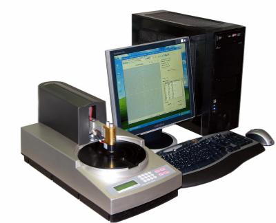
Under manual control, the front panel offers a user-friendly interface. Wafer information such as diameter, thickness, and measurement location can be input via the keypad. Results are displayed on the LCD readout. Connected to a PC, the CMT-SR2000N becomes a fully automated measurement system with an impressive array of measurement and output options. Point locations can be configured manually or selected from several pre-set maps including standard SEMI and ASTM configurations. Recipes can be created and stored for future use. CMT-SR2000NW software offers a variety of data analysis functions.
With pricing well below that of the competition, the CMT-SR2000N Automatic Mapping Four Point probe is an exceptional value. Specifications: Sheet resistance measurement
Resistivity measurement
Measurement Accuracy
Operating software
Measurement mode
Outside Dimensions
|
|
HOME ABOUT REPS NEW PRODUCTS SERVICES CONTACTS TECH TIPS LITERATURE WEB SITE MAP CALCULATORS Copyright 1999-2023 Materials Development Corporation All rights reserved
|